| 當前位置:首頁->方案設計 |
|
| MAX32630超低功耗高性能可穿戴MCU開發(fā)方案 |
|
|
| 文章來源: 更新時間:2016/5/4 15:33:00 |
在線咨詢: |
| |
Maxim公司的MAX32630/MAX32631是集成了浮點單元的超低功耗高性能ARM Cortex-M4F32位MCU,非常適合用于可穿戴醫(yī)療和健身設備.MCU組合了超低功耗高效率信號處理功能和大幅度降低功耗,使用方便.內部振蕩器工作高達96MHz,集成了2MB閃存, 512KB SRAM和8KB指令緩存,MCU內和工作電壓1.2V,I/O電壓1.8V-3.3V,主要用在健身監(jiān)視,手持醫(yī)療設備,傳感器集線器,運動手表和可穿戴醫(yī)療貼片.本文介紹了MAX32630主要特性,框圖和MAX3263x評估板優(yōu)勢和特性,框圖,電路圖,材料清單和PCB元件布局圖.
The MAX32630/MAX32631 is an ARM® Cortex® -M4F 32-bit microcontroller with a floating point unit, ideal for the emerging category of wearable medical and fitness applications. The architecture combines ultra-low power high-efficiency signal processing functionality with significantly reduced power consumption and ease of use. The device features four powerful and flexible power modes. A peripheral management unit (PMU) enables intelligent peripheral control with up to six channels to significantly reduce power consumption. Built-in dynamic clock gating and firmware-controlled power gating allows the user to optimize power for the specific application. Multiple SPI, UART and I²C serial interfaces, as well as 1-Wire® master and USB, allow for interconnection to a wide variety of external sensors. A four-input, 10-bit ADC with selectable references is available to monitor analog input from external sensors and meters. The small 100-ball WLP package provides a tiny, 4.37mm x 4.37mm footprint.
The MAX32630/MAX32631 include a hardware AES engine. The MAX32631 is a secure version of the MAX32630. It incorporates a trust protection unit (TPU) with encryption and advanced security features. These features include a modular arithmetic accelerator (MAA) for fast ECDSA, a hardware PRNG entropy generator, and a secure boot loader.
MAX32630主要特性:
High-Efficiency Microcontroller for Wearable Devices
Internal Oscillator Operates Up to 96MHz
Low Power 4MHz Oscillator System Clock Option for Always-On Monitoring Applications 2MB Flash Memory
512KB SRAM
8KB Instruction Cache
1.2V Core Supply Voltage
1.8V to 3.3V I/O
Optional 3.3V ±5% USB Supply Voltage
Power Management Maximizes Uptime for Battery Applications
106µA/MHz Active Current Executing from Cache
Wakeup to 96MHz Clock or 4MHz Clock
600nA Low Power Mode (LP0) Current with RTC Enabled
3.5µW Ultra-Low Power Data Retention Sleep Mode (LP1) with Fast 5µs Wakeup to 96MHz
Optimal Peripheral Mix Provides Platform Scalability
SPIX Execute in Place (XIP) Engine for Memory Expansion with Minimal Footprint
Three SPI Masters, One SPI Slave
Four UARTs
Three I²C Masters, One I²C Slave
1-Wire Master
Full-Speed USB 2.0 Engine with Internal Transceiver
Sixteen Pulse Train (PWM) Engines
Six 32-Bit Timers and 3 Watchdog Timers
Up to 66 General-Purpose I/O Pins
One 10-Bit Delta-Sigma ADC Operating at 7.8ksps
AES-64, -128, -256
CMOS-Level 32kHz RTC Output
Secure Valuable IP and Data with Robust Internal Hardware Security (MAX32631 Only)
Trust Protection Unit (TPU) Including MAA Supports ECDSA and Modular Arithmetic
PRNG Seed Generator
Secure Boot Loader
MAX32630應用:
Fitness Monitors
Portable Medical Devices
Sensor Hubs
Sports Watches
Wearable Medical Patches
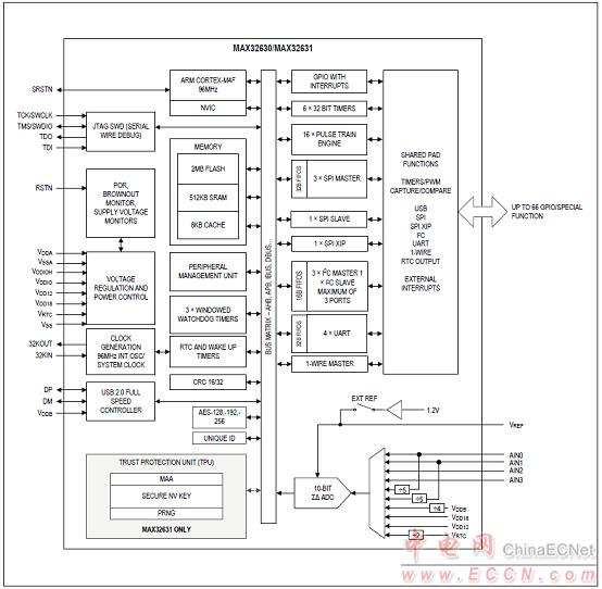
圖1.MAX32630簡化框圖
MAX3263x評估板
The MAX3263x evaluation kit (EV kit) provides a convenientplatform for evaluating the capabilities of theMAX3263x microcontroller. The EV kit also provides acomplete, functional system ideal for developing anddebugging applications.
MAX3263x評估板優(yōu)勢和特性:
●● Easily Load and Debug Code Using the SuppliedOlimex ARM-USB-TINY-H JTAG Debugger ConnectedThrough a Standard 20-Pin ARM JTAG Header
●● Selectable Power Sources for PMIC Include USBPower Through CN2, External Battery Through J2Connector, or Bench Supply Through Test PointsTP12 and TP13
●● Selectable Power Source for On-Board Peripherals(Switches, LEDs, OLED Display, SPI Flash,Bluetooth® LE Transceiver)
●● Headers for Accessing MAX3263X I/O Pins andAnalog Front End (AFE) Input Signals
●● USB Micro-B Connection to MAX3263x USB DeviceController
●● USB Micro-B Connection to USB-UART BridgeSelectable Between MAX3263x Internal UART 0 andUART 1
●● MAX3263X Internal Real-Time Clock (RTC)
●● On-Board Bluetooth 4.0 BLE Transceiver with ChipAntenna
●● General-Purpose Pushbutton Switches and IndicatorLEDs (All Connected to GPIOs) for User I/O
●● Prototyping Matrix (0.1in Grid) with Integrated PowerRails for Customer Circuitry
MAX3263x評估板包括:
●● EV kit board with a MAX3263X microcontroller
●● Olimex ARM-USB-TINY-H JTAG debugger with JTAGribbon cable (for connecting from debugger to EV kitheader J1) and USB standard A-to-B cable (for connectingfrom PC to debugger)
●● Standard-A to Micro-B USB cable (for connectingfrom PC or standalone USB power supply to EV kitUSB Micro-B connector CN2) allows connection fromPC USB host to MAX3263X USB device controllerperipheral
●● Standard-A to Micro-B USB cable (for connecting PCto EV dit USB connector CN1) allows virtual COMport interface to MAX3263X UART 0 or UART 1through a USB/UART bridge
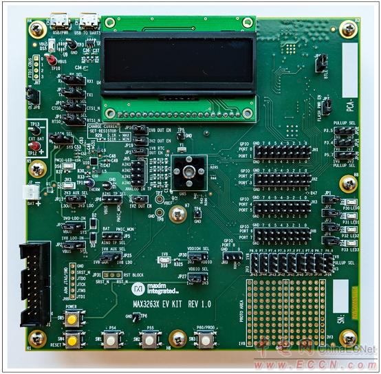
圖2.MAX3263x評估板外形圖
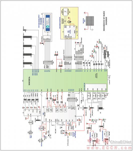
圖3.MAX3263x評估板框圖
圖4.MAX3263x評估板電路圖(1)
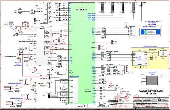
圖5.MAX3263x評估板電路圖(2)
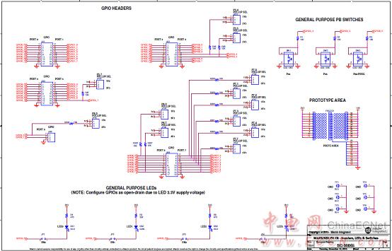
圖6.MAX3263x評估板電路圖(3)
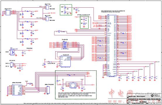
圖7.MAX3263x評估板電路圖(4)
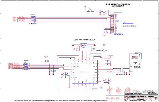
圖8.MAX3263x評估板電路圖(5)
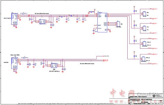
圖9.MAX3263x評估板電路圖(6)
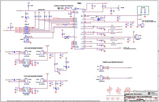
圖10.MAX3263x評估板電路圖(7)
MAX3263x評估板材料清單:
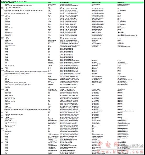

圖11.MAX3263x評估板PCB元件布局圖 |
| |
|
|
|
|
|
| |
|
| |
|
|
消息")