| ģĒ«įőĽ÷√£ļ ◊Ūď->ľľ–g(sh®ī)∑÷ŌŪ |
|
| MAX98357A PCM›Ē»ŽDÓź“ŰÓl∑Ňīů∆ųĹ‚õQ∑Ĺįł |
|
|
| őń’¬ĀŪ‘ī£ļ”ņł∑ŅĶŅ∆ľľ łŁ–¬ērťg£ļ2017/9/14 14:54:00 |
‘ŕĺÄ◊…‘É£ļ |
| |
MaximĻęňĺĶńMAX98357A/MAX98357B «ĒĶ(sh®ī)◊÷√}īa’{(di®§o)÷∆(PCM)›Ē»ŽDÓź∑Ňīů∆ų,ŐŠĻ©ABÓź“ŰÓl–‘ń‹ļÕDÓź–߬ ,”–őŚāÄŅ…ŖxďŮĶń‘Ų“ś‘O∂®(3dB, 6dB, 9dB, 12dBļÕ15dB),ÜőŽä‘ī2.5V-5.5VĻ§◊ų,5V 4¶łērĶń›Ē≥ŲĻ¶¬ ěť3.2W,–߬ 92% (RL = 8¶ł, POUT = 1W),›Ē≥Ų‘Ž“Ű25¶ŐVRMS (AV = 15dB),1kHzērĶńTHD+Něť0.015%,÷ų“™”√‘ŕĻP”õĪĺŽäńXļÕ…ŌĺW(w®£ng)Īĺ(Netbook), ÷ôCļÕ∆ĹįŚŽäńX.ĪĺőńĹťĹBŃňMAX98357A/MAX98357B÷ų“™Őō–‘,Ļ¶ń‹ŅÚąDļÕé◊∑NĎ™”√Žä¬∑,“‘ľįMAX98357ť_įl(f®°)įŚDEV(WLP)÷ų“™Őō–‘,ŅÚąD,Žä¬∑ąD,≤ńŃŌ«ŚÜőļÕPCB‘O”čąD.
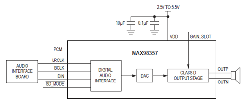
The MAX98357A/MAX98357B are digital pulse-code modulation (PCM) input Class D power amplifiers that provide Class AB audio performance with Class D efficiency. These ICs offer five selectable gain settings (3dB, 6dB, 9dB, 12dB, and 15dB) in I2S/left-justified mode set by a single gain select input and a fixed 12dB gain in TDM mode.
The digital audio interface is highly flexible with the MAX98357A supporting I2S data and the MAX98357B supporting left-justified data. Both ICs support 8 channel time division multiplexed (TDM) data. The digital audio interface accepts specified sample rates between 8kHz and 96kHz for all supported data formats. The ICs can be configured to produce a left channel, right channel, or (left/2 + right/2) output from the stereo input data. The ICs operate using 16/24/32-bit data for I2S and left-justified modes as well as 16-bit or 32-bit data using TDM mode. The ICs eliminate the need for the external MCLK signal that is typically used for PCM communication. This reduces EMI and possible board coupling issues in addition to reducing the size and pin count of the ICs.
The ICs also feature a very high wideband jitter tolerance (12ns typ) on BCLK and LRCLK to provide robust operation.Active emissions-limiting, edge-rate limiting, and overshoot control circuitry greatly reduce EMI. A filterless spread-spectrum modulation scheme eliminates the need for output filtering found in traditional Class D devices and reduces the component count of the solution.
The ICs are available in 9-pin WLP (1.345mm x 1.435mm x 0.64mm) and 16-pin TQFN (3mm x 3mm x 0.75mm) packages and are specified over the -40 °ś to +85°ś temperature range.
MAX98357A/MAX98357B÷ų“™Őō–‘:
Single-Supply Operation (2.5V to 5.5V)
3.2W Output Power into 4¶ł at 5V
2.4mA Quiescent Current
92% Efficiency (RL = 8¶ł, POUT = 1W)
25¶ŐVRMS Output Noise (AV = 15dB)
Low 0.015% THD+N at 1kHz
No MCLK Required
Sample Rates of 8kHz to 96kHz
Supports Left, Right, or (Left/2 + Right/2) Output
Sophisticated Edge Rate Control Enables Filterless Class D Outputs
77dB PSRR at 1kHz
Low RF Susceptibility Rejects TDMA Noise from GSM Radios
Extensive Click-and-Pop Reduction Circuitry
Robust Short-Circuit and Thermal Protection
Available in Space-Saving Packages: 1.345mm x 1.435mm WLP (0.4mm Pitch) and 3mm x 3mm TQFN
MAX98357A/MAX98357BĎ™”√:
Notebook and Netbook Computers
Cellular Phones
Tablets

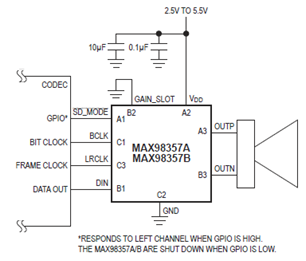
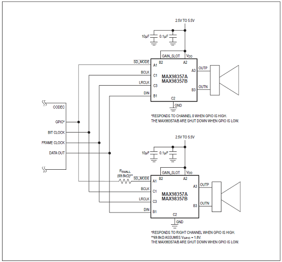
ąD1.MAX98357A/MAX98357BĻ¶ń‹ŅÚąD
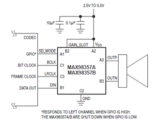
ąD2.MAX98357A/MAX98357B‘Ų“ś6dB◊ů¬∑PCMĻ§◊ųŽä¬∑
ąD3.MAX98357A/MAX98357B‘Ų“ś12dB◊ů¬∑PCMĻ§◊ųŽä¬∑
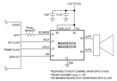
ąD4.MAX98357A/MAX98357B‘Ų“ś6dB”“¬∑PCMĻ§◊ųŽä¬∑

ąD5.MAX98357A/MAX98357B‘Ų“ś6dB(◊ů¬∑/2+”“¬∑/2)PCMĻ§◊ųŽä¬∑
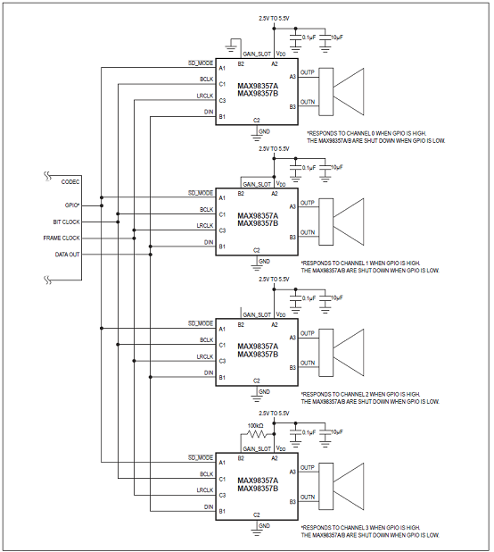
ąD6.MAX98357A/MAX98357B≤…”√É…āÄICĶńŃĘůw¬ēPCMĻ§◊ųŽä¬∑
ąD7.MAX98357A/MAX98357B‘Ų“ś12dBÕ®¬∑TDMĻ§◊ųŽä¬∑
MAX98357ť_įl(f®°)įŚDEV(WLP)
The MAX98357 development board (DEV board) is a fullyassembled and tested PCB that evaluates the MAX98357I2S digital input Class D power amplifier. The DEV boardoperates from a single 2.5V to 5.5V DC power supply andis capable of delivering 3.2W into a 4¶ł load. The deviceoutputs can be connected directly to a speaker load forfilterless applications. However, a filter can be added toease evaluation. The MAX98357A accepts standard I2Sdata and the MAX98357B accepts left-justified digital audio data. Both versions also support 8-channel TDMaudio data.
The MAX98357 evaluation system (EV system) includesthe MAX98357 DEV board and Maxim Integrated°Įs audiointerface board (AUDINT001 board).
The AUDINT001 board provides an easy-to-use USBaudio-to-I2S converter. This allows for any computer tobecome a digital audio source, which can be used toevaluate the devices. The AUDINT001 board can also beused to power the MAX98357. This allows for a completeevaluation from a single USB connection.
MAX98357ť_įl(f®°)įŚDEV(WLP)÷ų“™Őō–‘:
°Ů°Ů 2.5V to 5.5V Single-Supply Operation
°Ů°Ů Only a Single External Component (VDD Capacitor)Required in Many Applications
°Ů°Ů I2S, Left-Justified, or TDM Input
°Ů°Ů Five Selectable Gains (3db, 6dB, 9dB, 12dB, and15dB)
°Ů°Ů Audio Channel Select (Left, Right, and Mono Mix)
°Ů°Ů Filterless Operation
°Ů°Ů Optional Class D Output Filters for Ease ofEvaluation
°Ů°Ů Proven PCB Layout
°Ů°Ů Fully Assembled and Tested
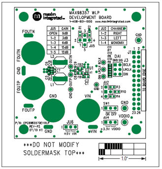
ąD8.MAX98357ť_įl(f®°)įŚDEV(WLP)ļÜĽĮŅÚąD
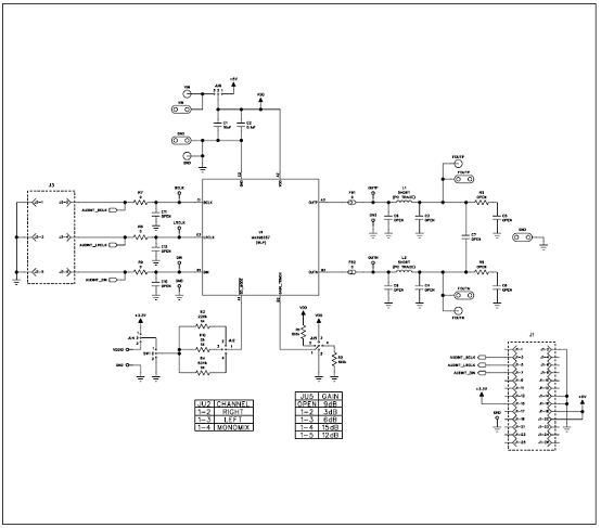
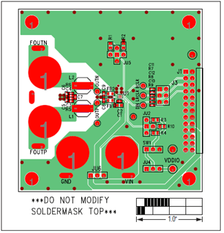
ąD9.MAX98357ť_įl(f®°)įŚDEV(WLP)Žä¬∑ąD
MAX98357ť_įl(f®°)įŚDEV(WLP)≤ńŃŌ«ŚÜő:
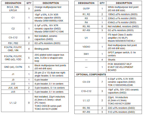
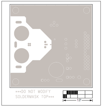
ąD10.MAX98357ť_įl(f®°)įŚDEV(WLP) PCB‘O”čąD(1)
ąD11.MAX98357ť_įl(f®°)įŚDEV(WLP) PCB‘O”čąD(2)
ąD12.MAX98357ť_įl(f®°)įŚDEV(WLP) PCB‘O”čąD(3)
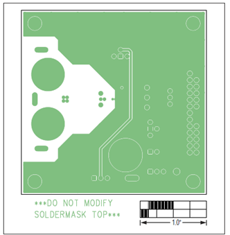
ąD13.MAX98357ť_įl(f®°)įŚDEV(WLP) PCB‘O”čąD(4)
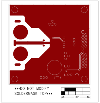
ąD14.MAX98357ť_įl(f®°)įŚDEV(WLP) PCB‘O”čąD(5) |
| |
|
|
|
|
|
| |
| |
| |
 |
ńķŅ…ń‹Ć¶“‘Ō¬ģa(ch®£n)∆∑ł–Ňd»§ |
 |
|
 |
| ģa(ch®£n)∆∑–ÕŐĖ |
Ļ¶ń‹ĹťĹB |
ľś»›–ÕŐĖ |
∑‚—b–ő Ĺ |
Ļ§◊ųŽäČļ |
āš◊Ę |
| CS8688 |
30W(4Ω£©+16W°Ń2(8Ω)/16V |
|
TSSOP-28 |
6.5V-18.5V |
Üő–ĺ∆¨2.1“ŰŌšĆ£”√DÓźĻ¶∑ŇIC |
| CS3816 |
2X15W/16V/8¶ł |
|
ESOP-16 |
6V-20V |
2°Ń15W √‚Žäł–ĶÕEMIŃĘůw¬ēDÓź“ŰÓlĻ¶¬ ∑ŇīůŽä¬∑,÷ß≥÷√‚Žäł–ļÕ∂ķôC›Ē≥ŲĎ™”√ |
|
| |
|
| |
|
|
ŌŻŌĘ")